Small lights with big potential: light emitting diodes & organic light emitting diodes
Commercial History (1960s - Today)
Introduction & Statistics
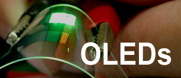
OLEDs - Introduction and How They Work
Inventors and Developments (LED)
Introduction:
The LED is a light source which uses semiconductors and electroluminescence to create light. There are two major kinds of light emitting diodes: LED and OLED. The LED is different than EL lamp in that it uses a small semiconductor crystal with reflectors and other parts to make the light brighter and focused into a single point. The OLED is very similar to the EL lamp in design, using a flat sandwich of materials. It is different than the LED and EL lamp in that it uses organic (carbon) molecules in the layer that emits light.All credits and sources are located at the bottom of each lighting page
Our video on LEDs and OLEDs, click the bracket icon on the lower right to expand size:
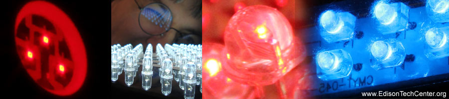
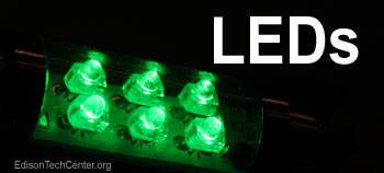
LEDs
Currently the LED lamp is popular due to it's efficiency and many believe it is a 'new' technology. The LED as we know it has been around for over 50 years. The recent development of white LEDs is what has brought it into the public eye as a replacement for other white light sources.
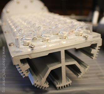
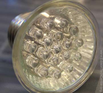
Common uses: indication lights on devices, small and large lamps, traffic lights, large video screens, signs, street lighting(although this is still not widespread)
Large LED array designed for use as a street lamp. A massive aluminum heat sink is needed with the high wattage LEDs
Advantages:
-Energy efficient source of light for short distances and small areas. The typical LED requires only 30-60 milliwatts to operate
-Durable and shockproof unlike glass bulb lamp types
-Directional nature is useful for some applications like reducing stray light pollution on streetlightsDisadvantages:
-May be unreliable in outside applications with great variations in summer/winter temperatures, more work is being done now to solve this problem
-Semiconductors are sensitive to being damaged by heat, so large heat sinks must be employed to keep powerful arrays cool, sometimes a fan is required. This adds to cost and a fan greatly reduces the energy efficient advantage of LEDs, it is also prone to failure which leads to unit failure
-Circuit board solder and thin copper connections crack when flexed and cause sections of arrays to go out
-Rare earth metals used in LEDs are subject to price control monopolies by certain nations
-Reduced lumen output over time
LED Statistics
*Lumens per watt: 28 - 150 (depends on environment)
*Lamp life: 25,000 - 100,000 hours
*CRI (White LEDs) - 70
*Color Temperature (White LEDs) - 2540 - 10,000K
*Available in 0.01 - 3 WLeft: White LEDs became an affordable commercial product in the 2000s
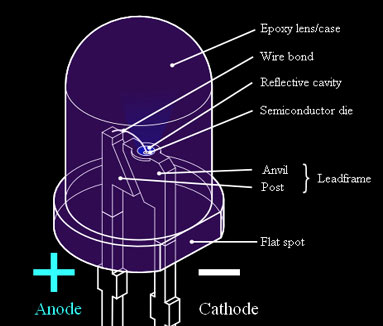
LEDs create light by electroluminescence in a semiconductor material. Electroluminescence is the phenomenon of a material emitting light when electric current or an electric field is passed through it - this happens when electrons are sent through the material and fill electron holes. An electron hole exists where an atom lacks electrons (negatively charged) and therefore has a positive charge. Semiconductor materials like germanium or silicon can be "doped" to create and control the number of electron holes. Doping is the adding of other elements to the semiconductor material to change its properties. By doping a semiconductor you can make two separate types of semiconductors in the same crystal. The boundary between the two types is called a p-n junction. The junction only allows current to pass through it one way, this is why they are used as diodes. LEDs are made using p-n junctions. As electrons pass through one crystal to the other they fill electron holes. They emit photons (light). This is also how the semiconductor laser works.
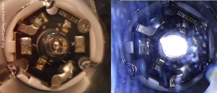
Above: A 5 Watt LED, one of the most powerful LEDs available.
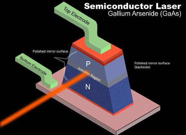
Above: A laser also creates light, but through a different construction. Read more about semiconductor devices used in electronics here.
To understand p-n junctions and semiconductors better you will need to invest a good amount of time in a lecture, it is not a simple phenomena and far too lengthy to cover here. See a 59 minute introduction lecture to solid state (semiconductors) here.
Phosphors are used to help filter the light output of the LED. They create a more pure "harsh" color.
Engineers had to figure out how to control the angle the light escapes the semiconductor, this "light cone" is very narrow. They figured out how to make light refract or bounce off all surfaces of the semiconductor crystal to intensify the light output. This is why LED displays traditionally have been best viewed from one angle.
Above: various colors of LEDs on display at the Edison Tech Center. The metal tabs on the sides of each help distribute the heat away from the LED.
Photo: Whelan Communications. Peter Heppner at the MTV music awards, Bucharest, RomaniaAbove: A "Jumbotron" or full color LED display. This type of display is only usable for large area applications and decorative backgrounds in small spaces. The human eye can only effectively perceive the image at more than 6 meters distance. The tricolor array is arranged in the close-up at the top right.
Colors:Red and Infrared LEDs are made with gallium arsenide
Bright Blue is made with GaN -gallium nitride
White LEDs are made with yttrium aluminum garnetThere are also orange, green, blue, violet, purple, ultraviolet LEDs.
For more details on elements used for each color go here.
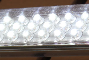
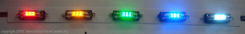
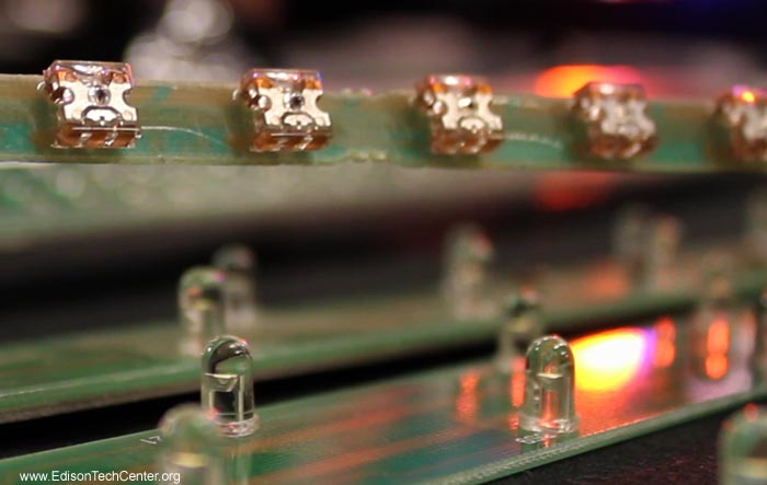
Above: Two different types of LEDs, both in a strip mount configuration

|
|
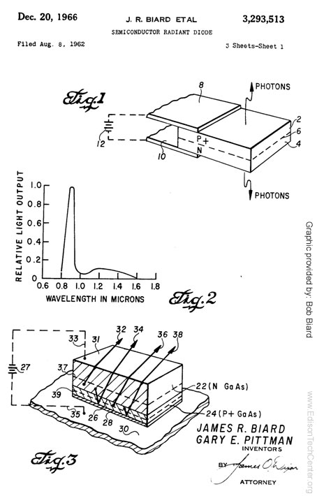
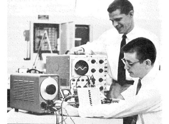
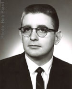
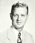
Above: 1958: Walter T. Matzen (top) and Bob Biard (bottom) worked on parametric amplifiers, this helped lay groundwork for the LED. Later Gary Pittman and Mr. Biard worked on varactor diodes which led to the LED as we know it. Read the full story of their work with this PDF here.
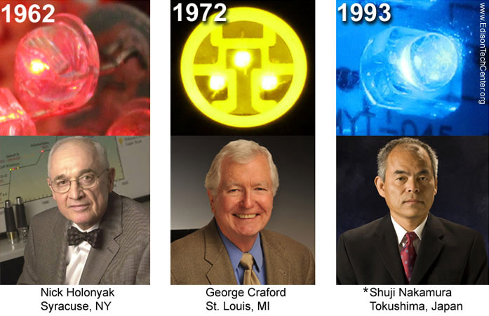
* 1972: Herbert P. Maruska & Jacques Pankove developed the violet LED which set the stage for development of a bright blue LED in 1993
Photos: Randy Lamb, UC Santa Barbara / Semicon West 2012 / PD-USGOV / Bob Biard
1907 - H.J. Round discovered electroluminescence when using silicon carbide and a cats whisker. Oleg Losev independently discovered the phenomena the same year.
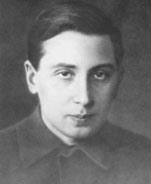
London, United Kingdom1920s - Oleg V. Losev studied the phenomena of light emitting diodes in radio sets. His first work on 'LEDs' involved a report on light emission from SiC. In 1927 he published a detailed report but his work was not well known until the 1950s when his papers resurfaced.
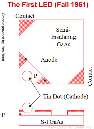
Saint Petersburg, Russia1961 - James R. Biard. "Bob" Biard and Gary Pittman developed the Infrared LED at Texas instruments. This was the first modern LED. It was discovered by 'accident' while TI tried to make an X-band GaAs varactor diode. The discovery was made during a test of a tunnel diode using a zinc diffused area of a GaAs (Gallium Arsenide) semi-insulating substrate.
Dallas, TexasPhoto: Robert Biard
1961 - Gary Pittman worked together with James R. Biard. He had started working in 1958 with semiconductor GaAs for the creation of early solar cells. He discovered and developed the infrared LED with James R. Biard.
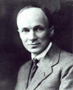
Dallas, Texas1962 - Nick Holonyack Jr. develops the red LED, the first LED of visible light. He used GaAsP (Gallium Arsenide Phosphide) on a GaAs substrate. General Electric.
Syracuse, New YorkPhoto: PD-USGOV
1972 - M. George Craford creates the first yellow LED at Monsanto using GaAsP. He also develops a brighter red LED.
St. Louis, MissouriPhoto: Semicon West 2012
1972 - Herbert Maruska and Jacques Pankove develop the violet LED using Mg-doped GaN films. The violet LED is the foundation for the true blue LED developed later.
RCA Labs , New Jersey
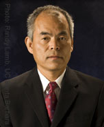
1979 - Shuji Nakamura develops the world's first bright blue LED using GaN (Gallium nitride). It wouldn't be until the 1990s that the blue LED would become low cost for commercial production.
Tokushima, JapanPhoto: Randy Lamb, UC Santa Barbara
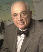
1976 - Thomas P. Pearsall develops special high brightness LEDs for fiber optic use. This improves communications technology worldwide. Paris, France
Photo: T.P. Pearsall
What is an OLED?
The Organic LED is made of a layer of organic electroluminescent material with p/n junction sandwiched between to electrodes. At least one of the electrodes is transparent so the photons can escape. Similar to an EL lamp, current is passed through a semiconductor (like the phosphor in an EL lamp), however the difference is that an OLED uses a p/n junction were there is a recombination of p and n carriers. EL (TDFEL, TFEL, powder EL) technology only uses a material excited by current to make light.
The semiconductor in an OLED is organic which means it contains carbon. The OLED uses one of two kinds of compounds: polymers or 'small molecule'. Read more about how it works below.
Uses:
Lamps - short distance indoor lamps (produces a diffused light)
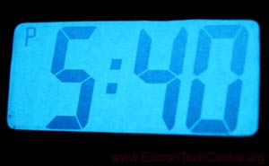
Displays - small: phones and media devices and large: televisions, computer monitors
Advantages:
-The units are lighter than traditional LEDs and can be made thinner as well
-OLEDs can provide a more energy efficient alternative to LCD computer and television monitors
-Can be used in a myriad of new applications in which lighting technology has never been used before
Disadvantages:
-The cost of OLEDs is still high and each unit produces less lumens than a normal LED
-The technology is still under development so the life of the OLED is being researched as new materials are used and tested each year. Until more research is done we will not know how these lamps with new materials compare with established technology.
OLED Statistics
*Lumens per watt: up to 50 in lamps (as of 2/2012)
*Lamp life: still under research
*CRI (White OLEDs) - still under research
*Color Temperature (White LEDs) - various whites are in development
*Available wattage: N/A
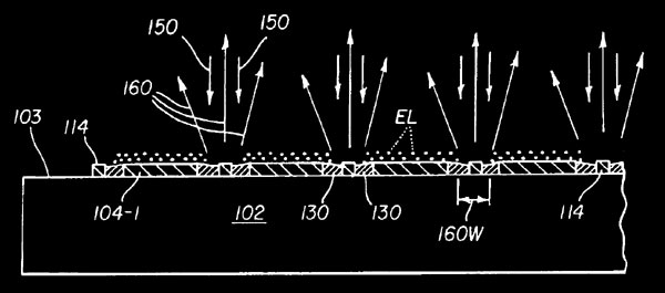
Patent by OLED co-inventor Stephen Van SlykeDisplays (computer monitors, televisions, mobile phone screens):
The OLED display is made by using multiple layer construction along with transistors which control whether each pixel is on or off. This is very similar to EL displays. The OLED display has the potential to be more efficient and thinner than the LCD. One advantage is that does not need a cold cathode fluorescent backlight like an LCD. The lack of a backlight means it can better display blacks (the back light always seeps through in black areas of the screen). The OLED display can also provide better contrast ratios than an LCD. The OLED display may also be made into a thin flexible material which could roll up like a newspaper. Currently the OLED is not as bright as EL or LCD displays it works better in areas with less ambient light. That may change as engineers work to increase luminosity.
Below: our simple video on OLED use in monitors and smart phones:
The diagram above is a simple modern OLED. There are a many new ways to construct the OLED using a variety of layer configurations. Displays will have additional layers such as an active matrix TFT (thin film transistor) which control pixel regions.Layers:
Early OLEDs had one layer of organic material between two electrodes.
Modern OLEDs are bi-layer, they have an emissive layer and conductive layer sandwiched between two electrodes (see diagram above).1. Electric current passes from the cathode to the anode. It passes through two layers of organic molecules.
2. The first layer the electrons pass into what is called the emissive layer. Electrons leave the conductive layer making 'holes' (positive charge). Meanwhile in the emissive layer there are excessive electrons (negative). The 'holes' jump to the emissive layer along the border of the two layers where they recombine with electrons (this place is the p/n junction). When the electrons join the holes light is emitted.
Light color is dependent on the materials used in the organic or polymer layers
Photo: Wikipedia: Tobias G.Types of OLEDs:
LEC - Electrochemical Cell - this has ions added to the OLED
PMOLED - Passive-matrix OLED - the first display technology, developed in the mid 90s
AMOLED - Active-matrix OLED - used in displays, it has a switch built into it in the form of a thin film transistor backplane. The transistor allows the unit to be switched on and off.
PLED - polymer LED
Polymer LEDs use a plastic to emit light. They have the properties of semiconductors yet are versatile and low cost to produce. The layers that emit light are similar to an ink and will be very cheap to manufacture once stable compounds and processes are developed.Deeper understanding of these improvements requires a basic background in chemistry and physics, you also can read more detail here.
The Future:
OLEDs will allow for thinner TV and computer displays, transparent "heads up" displays, flexible displays, flat roll-on surface lights on the sides of buildings or vehicles, changing camouflage displays for military vehicles, new photovoltaic applications, and much more. We can expect a lower production cost compared to LEDs due to less part assembly. At the moment OLEDs need more lab work to reach full potential.
Carbon nanotube technology is being developed for use with the OLED.
1979, 1987- Ching Tang discovers that he can create light by sending current through a carbon material. Steven Van Slyke and Tang built the first OLED at Kodak in 1987. Later he works on an OLED displays. His first light was a bright green light at 10 volts. Ching Tang continues to work on OLEDs at the University of Rochester.
Rochester, New YorkPhoto: University of Rochester
1979, 1987- Steven Van Slyke worked with Ching Tang on the first OLEDs at Kodak. Kodak becomes a patent holder of SMOLED (small-molecule OLED) technology. SMOLED requires depositing organic molecules in a vacuum. This is a very expensive process at the time.
Rochester, New YorkPhoto: Steven Van Slyke
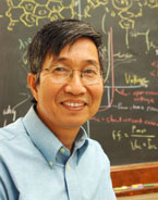
1988 - Chihaya Adachi invented electron transport materials and constructed a double heterostructure OLED which has been widely used in present OLEDs. Since 1988, his research has been focusing on material development and device physics. Recently he invented 3rd generation light emitting materials, TADF, enabling efficient EL. Read from his papers
Fukuoka, Japan
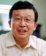
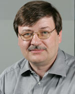
Photo: Chihaya Adachi1988 - Tetsuo Tsutsui contributed much to the development of high-performance OLEDs through the proposals of design concept on multilayer OLEDs in 1988, the concept of carier balance in 1992, and the usage of the optical microcavity effect in 1993. Testuo Tsutsui with Prof. Shogo Saito made many contributions to the commercialization of small-size OLED displays by Pioneer, TDK and Sanyo Electric in Japan.
Fukuoka , Japan Photo: Prof. Tetsuo Tsutsui1990 - Jeremy Burroughes along with Richard Friend and Donal Bradley discover polymer based OLEDs, this reduced cost of production to marketable levels. PLED (polymer LED) technology competes with SMOLED for the future of OLEDs. Cambridge University Cavendish Laboratory. Read More.
Cambridge, United KingdomPhoto: Jeremy Burroughes
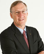
1990 - Richard Friend - PLED developer at Cambridge University Cavendish Laboratory. The polymer LED is cheaper to produce than SMOLED because it does not use vacuum deposition. Thin films can be deposited on larger sheets. This is a step towards the later development of OLED displays.
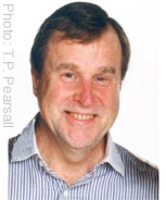
Cambridge, United Kingdom1990 - Donal Bradley - Used poly(para-phenylenevinylene), PPV, ~100 nm thick between indium oxide and aluminum layers to create the conjugated polymer LED reported in Nature in 1990. This had a yellow-green colored light. Quantum efficiency: 0.05%. Subsequently developed high efficiency polyfluorene PLEDs at Sheffield University with Dow Chemical Company. Donal Bradley now leads the Centre for Plastic Electronics at Imperial College London, working in collaboration with Sumitomo Chemical Company on PLEDs for displays, lighting and lasers. See useful links on Bradley's work on Useful Links below.
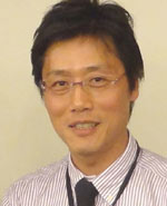
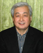
London, United Kingdom Photo: Imperial College, London1997 - Teruo (Ted) Tohma developed the first commercial OLED displays using PMOLED (passive matrix organic LED) technology at Pioneer. He also envisioned the move from PMOLED to AMOLED and later developed a p-Si active matrix displays. The AMOLED is first sold in 2007.
Tokyo, Japan
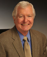
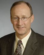
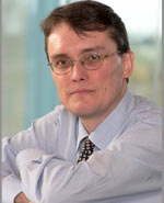
Photo: Ted Tohma1998 - Stephen R. Forrest advanced OLED research, and continues to work on development. In 1998 Forrest and Thompson built the first phosphorescent OLED.
Los Angeles, CaliforniaPhoto: University of Michigan
1998 - Mark E. Thompson and Stephen Forrest develop the first phosphorescent OLED (PHOLED) by using an emissive later of platinum(II) octaethylporphyrin. The PHOLED is more efficient than a normal fluorescent LED. They developed green and red OLEDs using iridium. The PHOLED is still not commercialized. University of Southern California.
Los Angeles, California
Photo: Mark E. Thompson2021 - You - Choose engineering for your career! Work on fascinating new technologies, make new breakthroughs in lighting and change our world for the better. LEARN MORE HERE
Timeline of major events:
1979 - Discovery of organic electroluminescent materials, Kodak
1987 - First organic light emitting diode built at Kodak
1990 - First PLEDs discovered, Cambridge University
1997 - First commercial PMOLED displays produced at Pioneer
1998 - First phosphorescent OLED developed
2007 - Samsung Mobile Display develops the first commercial AMOLED (active matrix organic LED) display.Lamps are presented in the order of chronological development
Previous: Electroluminescent Lamp 1958
Next: Metal Halide Lamp 1962


Help us expand and improve our learning material by volunteering or by donation.
![]()
COMMENTS?
Help us edit and add to this page by becoming a ETC volunteer!
Give us feedback on this and other pages using email
or our Facebook
Page
Useful Links, More Resources:
LEDs:
OLEDs:
The PLED: Donal Bradley, Jeremy Burroughes and Richard Friend:
Nature paper highlighted in: www.nature.com/physics/looking-back
(This is the most highly cited paper in the field. DDCB was corresponding author.)
Royal Society Bakerian Lecture: http://royalsociety.org/royalsociety.tv/?from=footer
(Freely viewable on-line)
Another RS video on plastic electronics: http://www.youtube.com/watch?v=0D_W_q1a0vU
Centre for Plastic Electronics Homepage: http://www3.imperial.ac.uk/plasticelectronics
DDCB Home page: http://www3.imperial.ac.uk/people/d.bradley
The First Practical LED by Thomas Okon and Bob Biard
Website, graphics and article by M. Whelan
Thanks to assistance from Bob Biard, Chihaya Adachi, Chris King, Donal
Bradley, Tetsuo Tsutsui and Ted Tohma
Sources/References:
University of Rochester
Wikipedia: LED, Electron Hole, YAK, OLEDs
Edison Tech Center: Interview with Robert N. Hall
Interview with John D. Harnden Jr.
Also thanks to information provided by Jeremy Burroughes, Robert Biard
oled-info.com
businesswire.com/news
cnx.org
Donal Bradley
US Patents: 67794676 Pakbaz
Chihaya Adachi
Contributions of Prof. Tetsuo Tsutsui in R&D of OLED technology
H. Maruska
James R. Biard
Photos:
Edison Tech Center
Whelan Communications
US Government
Semicon West
UC Santa Barbara
T.P. Pearsall
University of Rochester
University of Michigan
J. Robert Biard
Steve Van Slyke
Jeremy Burroughes
Imperial College, London
Ted Tohma
Chihaya Adachi
Tetsuo Tsutsui
Photo/Video
use:
Commercial entities must pay for use of photos/graphics/videos in their
web pages/videos/publications
No one commercial or public is allow to alter Edison Tech Center photos/graphics/videos.
Educational Use: Students and teachers may use photos and videos
for school. Graphics and photos must retain the Edison Tech Center watermark
or captions and remain unmanipulated except for sizing.
Permissions
- Videos: We do not email, FTP, or send videos/graphics to anyone
except in DVD form. Payment is needed for this service. See our donate
page for pricing, and our catalogue
for a listing of videos on DVD.
Professional video production companies may get videos in data form with
signed license agreements and payment at commercial rates.
Back
to Home
Copyright
2013 Edison Tech Center